- 您现在的位置:买卖IC网 > Sheet目录1227 > MAX16929EVKIT+ (Maxim Integrated Products)KIT EVALUATION FOR MAX16929
�� �
�
�MAX16929�
�Automotive� TFT-LCD� Power� Supply� with� Boost�
�Converter� and� Gate� Voltage� Regulators�
�Table 3. Compensation Component Values�
�V� SH � (V)� 8� 18�
�I� SH � (mA)� 200� 200�
�V� INA � (V)� 3.3� 5�
�55� F� A� and� the� resulting� gate� source� voltage� (V� GS� )� turns�
�on� the� FET.� When� the� gate� drive� is� removed� under� a� fault�
�condition� or� in� shutdown,� R� SG� bleeds� off� charge� to� turn�
�off� the� FET.� Size� R� SG� to� produce� the� V� GS� needed� to� turn�
�on� the� FET.�
�P� IN � (W)�
�L (μH)�
�R� COMPV� (k� I� )�
�C� COMPV� (pF)�
�C� COMPI� (pF)�
�V� SH�
�LXP�
�1.75�
�5�
�33�
�220�
�820�
�3.75�
�5�
�39�
�180�
�330�
�V� CP�
�1.8V/3.3V� Regulator� Controller�
�npn� Bipolar� Transistor� Selection�
�There� are� two� important� considerations� in� selecting� the�
�pass� npn� bipolar� transistor:� current� gain� (h� FE� )� and� power�
�dissipation.� Select� a� transistor� with� an� h� FE� high� enough� to�
�ensure� adequate� drive� capability.� This� condition� is� satis-�
�fied� when� I� DR� x� (h� FE� +� 1)� is� greater� than� the� maximum�
�load� current.� The� regulator� can� source� I� DR� =� 4.5mA� (min).�
�The� transistor� should� be� capable� of� dissipating:�
�P� NPN_REG� =� (V� INA� -� V� REG_OUT� )� � I� LOAD(MAX)�
�where� V� REG_OUT� =� 1.8V� or� 3.3V.� Bypass� DR� to� ground�
�with� a� 0.1� F� F� ceramic� capacitor.� For� applications� in� which�
�the� boost� output� current� exceeds� 300mA,� connect� a�
�30k� I� resistor� from� DR� to� ground.�
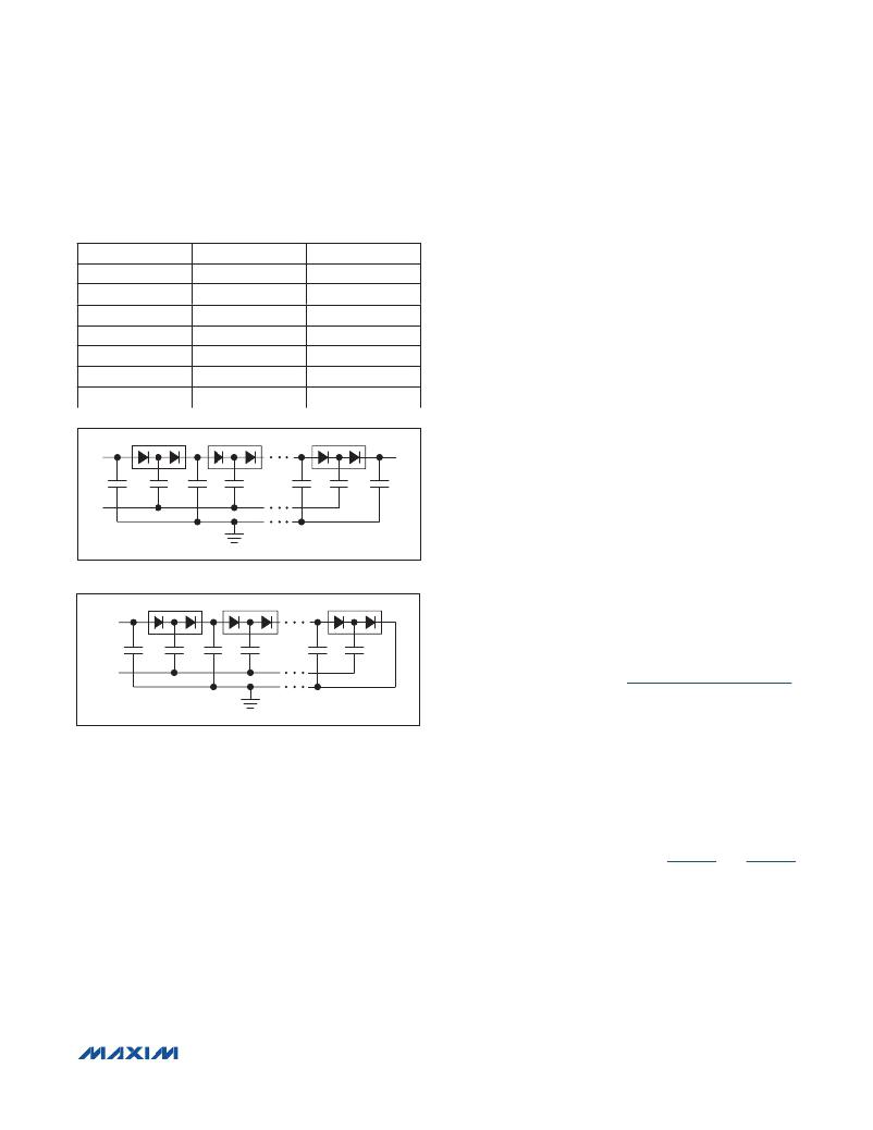
�Figure� 2.� Multistage� Charge� Pump� for� Positive� Output� Voltage�
�V� CN�
�LXP�
�Figure� 3.� Multistage� Charge� Pump� for� Negative� Output� Voltage�
�To� further� optimize� transient� response,� vary� R� COMPV�
�in� 20%� steps� and� C� COMPV� in� 50%� steps� while� observ-�
�ing� transient-response� waveforms.� The� ideal� transient�
�response� is� achieved� when� the� output� settles� quickly� with�
�little� or� no� overshoot.� Connect� the� compensation� network�
�to� the� analog� ground� plane.�
�Use� the� following� formula� to� calculate� the� value� for� C� COMPI� :�
�C� COMPI� ≤� 950� ×� 10� -6� ×� L/(V� SH� +� V� SCHOTTKY� -� V� INA� )�
�p-Channel� FET� Selection�
�The� p-channel� FET� used� to� gate� the� boost� converter’s�
�input� should� have� low� on-resistance.� Connect� a� resistor�
�(R� SG� )� between� the� source� and� gate� of� the� FET.� Under�
�normal� operation,� R� SG� carries� a� gate� drive� current� of�
�Supply� Considerations�
�INA� needs� to� be� at� least� 4.5V� for� the� 3.3V� regulator� to�
�operate� properly.�
�Charge� Pumps�
�Selecting� the� Number� of� Charge-Pump� Stages�
�For� most� applications,� a� single� charge-pump� stage� is�
�sufficient,� as� shown� in� the� Typical Application Circuit� .�
�Connect� the� flying� capacitors� to� LXP.� The� output� voltages�
�generated� on� the� storage� capacitors� are� given� by:�
�V� CP� =� 2� x� V� SH� +� V� SCHOTTKY� -� 2� x� V� D�
�V� CN� =� -(V� SH� +� V� SCHOTTKY� -� 2� x� V� D� )�
�where� V� CP� is� the� positive� supply� for� the� positive-gate� volt-�
�age� regulator,� and� V� CN� is� the� negative� supply� for� the� neg-�
�ative-gate� voltage� regulator.� Where� larger� output� voltages�
�are� needed,� use� multistage� charge� pumps� (however,� the�
�maximum� charge-pump� voltage� is� limited� by� the� absolute�
�maximum� ratings� of� CP� and� DRVN).� Figure 2� and� Figure 3�
�show� the� configuration� of� a� multistage� charge� pump� for�
�both� positive� and� negative� output� voltages.�
�For� mutistage� charge� pumps� the� output� voltages� are:�
�V� CP� =� V� SH� +� n� � (V� SH� +� V� SCHOTTKY� -� 2� x� V� D� )�
�V� CN� =� -n� � (V� SH� +� V� SCHOTTKY� -� 2� x� V� D� )�
�For� highest� efficiency,� choose� the� lowest� number� of�
�charge-pump� stages� that� meets� the� output� requirement.�
� ????????????????????????????????????????????????????????????????� � Maxim� Integrated� Products� � � 18�
�发布紧急采购,3分钟左右您将得到回复。
相关PDF资料
MAX16946EVKIT+
KIT EVALUATION FOR MAX16946
MAX17015EVKIT+
KIT EVAL FOR MAX17015
MAX17021EVKIT+
EVAL KIT FOR MAX17021
MAX1702EVKIT
EVAL KIT FOR MAX1702
MAX17710EVKIT#
RD ENERGY HARVESTING
MAX19000EVKIT+
EVAL KIT MAX19000
MAX19710EVKIT+
EVAL KIT FOR MAX19710
MAX1978EVKIT
EVAL KIT MAX1978
相关代理商/技术参数
MAX16929FGUI/V+
功能描述:LCD 驱动器 18V 2MHz Auto TFT-LCD Pwr Supply RoHS:否 制造商:Maxim Integrated 数位数量:4.5 片段数量:30 最大时钟频率:19 KHz 工作电源电压:3 V to 3.6 V 最大工作温度:+ 85 C 最小工作温度:- 20 C 封装 / 箱体:PDIP-40 封装:Tube
MAX16929FGUI/V+T
功能描述:LCD 驱动器 18V 2MHz Auto TFT-LCD Pwr Supply RoHS:否 制造商:Maxim Integrated 数位数量:4.5 片段数量:30 最大时钟频率:19 KHz 工作电源电压:3 V to 3.6 V 最大工作温度:+ 85 C 最小工作温度:- 20 C 封装 / 箱体:PDIP-40 封装:Tube
MAX16929GGUI/V+
功能描述:LCD 驱动器 18V 2MHz Auto TFT-LCD Pwr Supply RoHS:否 制造商:Maxim Integrated 数位数量:4.5 片段数量:30 最大时钟频率:19 KHz 工作电源电压:3 V to 3.6 V 最大工作温度:+ 85 C 最小工作温度:- 20 C 封装 / 箱体:PDIP-40 封装:Tube
MAX16929GGUI/V+T
功能描述:LCD 驱动器 18V 2MHz Auto TFT-LCD Pwr Supply RoHS:否 制造商:Maxim Integrated 数位数量:4.5 片段数量:30 最大时钟频率:19 KHz 工作电源电压:3 V to 3.6 V 最大工作温度:+ 85 C 最小工作温度:- 20 C 封装 / 箱体:PDIP-40 封装:Tube
MAX16929GUI/V+
功能描述:LCD 驱动器 18V 2MHz Auto TFT-LCD Pwr Supply RoHS:否 制造商:Maxim Integrated 数位数量:4.5 片段数量:30 最大时钟频率:19 KHz 工作电源电压:3 V to 3.6 V 最大工作温度:+ 85 C 最小工作温度:- 20 C 封装 / 箱体:PDIP-40 封装:Tube
MAX16929GUI/V+T
功能描述:LCD 驱动器 18V 2MHz Auto TFT-LCD Pwr Supply RoHS:否 制造商:Maxim Integrated 数位数量:4.5 片段数量:30 最大时钟频率:19 KHz 工作电源电压:3 V to 3.6 V 最大工作温度:+ 85 C 最小工作温度:- 20 C 封装 / 箱体:PDIP-40 封装:Tube
MAX16929HGUI/V+
功能描述:LCD 驱动器 18V 2MHz Auto TFT-LCD Pwr Supply RoHS:否 制造商:Maxim Integrated 数位数量:4.5 片段数量:30 最大时钟频率:19 KHz 工作电源电压:3 V to 3.6 V 最大工作温度:+ 85 C 最小工作温度:- 20 C 封装 / 箱体:PDIP-40 封装:Tube
MAX16929HGUI/V+T
功能描述:LCD 驱动器 18V 2MHz Auto TFT-LCD Pwr Supply RoHS:否 制造商:Maxim Integrated 数位数量:4.5 片段数量:30 最大时钟频率:19 KHz 工作电源电压:3 V to 3.6 V 最大工作温度:+ 85 C 最小工作温度:- 20 C 封装 / 箱体:PDIP-40 封装:Tube